
TSMC might not be raising 2nm wafer prices as much as thought
A diagram of a gate-all-around transistor. | Image credit-nist.gov
TSMC wafer prices for chips made in the U.S. will carry a premium
The Taiwan-based Investors.com says that 3nm wafers are currently priced at $25,000-$27,000; that will make the hike to $30,000 a 10% to 20% increase instead of the 50% increase previously calculated. The report also states that the manufacturing of chips using advanced nodes (3nm, 4nm, 5nm, 6nm, and 7nm) are running at full capacity. Production facilities for Legacy nodes such as 28nm, 40nm, 65nm, and 90nm are said to be underutilized.
Chips made at TSMC’s U.S. facilities will carry a 5% to 20% premium according to AMD CEO Lisa Su. Other reports say that the current production of 4nm chips from TSMC’s current operational fab in Arizona carries a 30% premium. With its overseas fabs reducing TSMC’s gross margins by 2% to 3%, TSMC feels that it must raise its prices at its U.S. fabs in order to keep its gross profit margin at 53%. That’s the target TSMC has for this financial metric so that the company can generate enough profits to continue investing in its business.
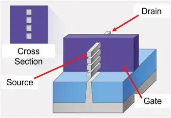
TSMC’s 2nm node introduces a new transistor
The 2nm node introduces a new type of transistor called Gate-All-Around (GAA). By using horizontal stacks of vertical nanosheets, the gate covers all four sides of the channel preventing current leaks and improving the drive current. This improves the performance and the energy-efficiency of the chip.
One of TSMC’s major clients, Nvidia, has backed the foundry’s price hike. Jensen Huang, co-founder and CEO of the most valuable publicly traded U.S. company, said, “The value of what TSMC produces is very high… a price increase is natural and consistent with the value they deliver.” Furthermore, Huang calls TSMC “one of the greatest companies in the history of humanity.”
For the second quarter of 2025, TSMC had a record high market share in the contract foundry industry of 70.3%. That is a huge lead over second place Samsung Foundry and its 7.3% Q2 2025 share.
After 2nm, TSMC expects to mass produce A16 chips. The A stands for angstroms with 1 nanometer equaling 10 angstroms. Thus, 16 angstroms will be equivalent to 1.6nm. This new node will start being employed in 2026 and will use the new Super Power Rail feature which is the foundry’s version of Backside Power Delivery. Instead of placing powerlines on the top of a wafer, they will be placed on the back of the wafer. This could generate an 8% to 10% improvement in the speed of a chip along with a 15% to 20% reduction in power consumption at the same speed.
The A16 node is expected to be followed up with high volume manufacturing using A14 (1.4nm) in 2028.

“Iconic Phones” is coming this Fall!
Good news everyone! Over the past year we’ve been working on an exciting passion project of ours and we’re thrilled to announce it will be ready to release in just a few short months.
LEARN MORE AND SIGN UP FOR EARLY BIRD DISCOUNTS HERE
#Latest #rumor #TSMCs #wafers #2nm #APs #great #news #phone #buyers