EUV machines cost $150 million and up. They are built by only one company in the world
Before EUV Lithography was created, there was Deep Ultraviolet (DUV) lithography which had a longer 193 nm wavelength. DUVs allowed foundries to manufacture chips using a process node as low as 10nm and the EUV has been employed to produce an Integrated Circuit (IC) at process nodes of 7nm, 5nm, 3nm, and 2nm. As process node numbers drop, transistor sizes drop allowing more of them to fit inside a chip. The more transistors inside an IC, the more powerful and energy-efficient it becomes.
The current price of an EUV is $150 million-$200 million for the Low-NA EUV. The production of future cutting-edge chips will require the latest generation of EUV machines, the High-NA EUV, which costs $350 million to $380 million. The latter has a Numerical Aperture of .55 compared to .33 for the former. This gives the High-NA machine the ability to print smaller features (like circuitry patterns) in greater resolution.
Without the High-NA EUV machine, foundries will have to use a technique called multi-patterning which involves dividing the design into multiple patterns that are a printed multiple times. This could lead to poor yields as there needs to be perfect alignment before each exposure to make it work.
There is only one company in the world that builds EUV machines, Dutch firm ASML. The company has followed U.S. sanctions and has kept EUV lithography out of China. It might not help the Chinese produce cutting-edge chips, but an American start-up company named Substrate has developed X-ray Lithography (XRL) technology that delivers a light source based on particle acceleration.
Substrate hopes to extend Moore’s Law into the future
That’s when the speed and energy of subatomic particles (like protons, electrons, and ions) are increased to nearly the speed of light using particle accelerators. Substrate says it aims to deliver resolutions that match ASML’s 2nm-class process. The company says that its products will be cheaper to run than the competition and will offer finer resolutions before 2030.


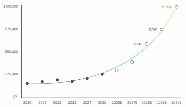
Chart shows past, current, and expected future silicon wafer prices for cutting-edge chips. | Image credit-Substrate
Substrate says that “Our accelerators create and power beams that generate light billions of times brighter than the sun, directly into our lithography tools, each using a completely new optical and high-speed mechanical system to produce the smallest of features needed for advanced semiconductor chips. While current approaches are reaching their limits, leading to increasing costs and complexity, all of our inventions are designed to work together to extend Moore’s Law for years to come.”
Moore’s Law is the observation made by Intel co-founder Gordon Moore that says transistor density on integrated circuits double every other year. Transistor density measures the number of transistors per square millimeter. What Substrate is saying is that its X-ray Lithography (XRL) will work for future process nodes and more complex designs.
Substrate is returning the U.S. to dominance in semiconductor production
We’ve never told you about Rock’s law which says that the cost of building a leading-edge semiconductor fabrication facility doubles every four years. For example, such a facility cost $5 billion in the early 2010s and costs about $25 billion today.
Substrate says that by 2030, wafers will cost $100,000 each compared to the current $30,000 for 2nm wafers. Fabs will cost over $50 billion each. According to Substrate, in this scenario “only the largest companies will be able to afford to build products that leverage leading-edge silicon. The economics of this scaling are more daunting than the physics. This economic model feels broken.”
This is where Substrate comes in. The company’s website says that it has a “pathway” to reduce the expense of manufacturing cutting-edge chips. By the end of the decade, Substrate says it will produce wafers costing end-users closer to $10,000 than $100,000. And as good for the semiconductor industry as it might be, Substrate says its technology is also “Returning the United States to dominance in semiconductor production.”
#Major #chipmaking #breakthrough #aimed #returning #U.S #dominance #chip #production
